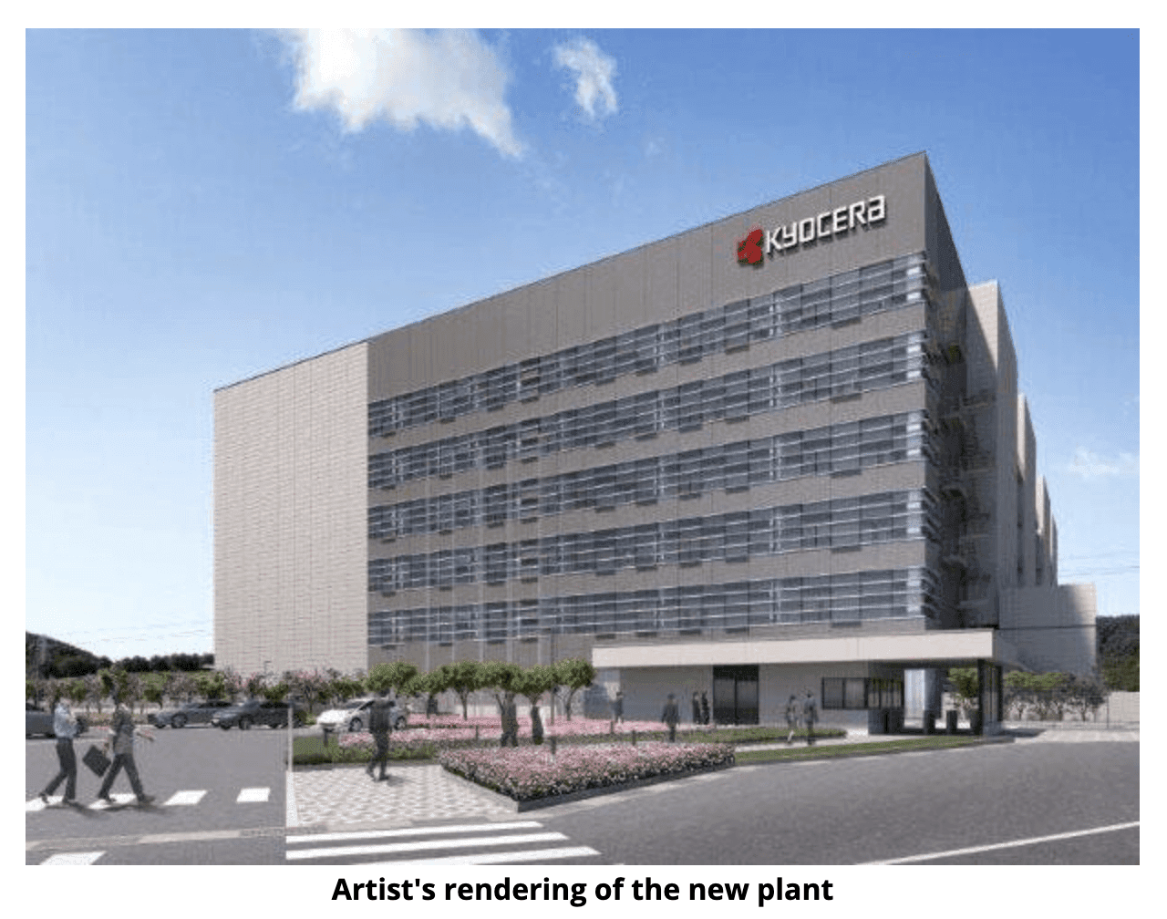
Kyocera's new Nagasaki plant, focusing on semiconductor components, signals a broader trend in high-tech manufacturing and its implications for future e-waste streams.
Kyocera Corporation officially opened its new Nagasaki Isahaya Plant on September 4, 2026, a facility dedicated to manufacturing critical components for the semiconductor industry.
This significant investment in advanced manufacturing signals Kyocera's strategic response to global demand for semiconductors, directly impacting the volume and complexity of future e-waste streams and requiring recyclers to adapt to new material compositions.
Kyocera's Strategic Expansion in Semiconductor Manufacturing
The new Nagasaki Isahaya Plant represents a substantial expansion of Kyocera's production capacity for ceramic packages and organic packages, essential components for high-performance semiconductors. This move aligns with a broader industry trend of reshoring and increasing domestic production capabilities in key technological sectors, driven by supply chain vulnerabilities and geopolitical considerations. The plant incorporates advanced automation and aims for high energy efficiency in its operations.
- Kyocera invested ¥100 billion ($680 million USD) in the new facility.
- The plant is located in Isahaya City, Nagasaki Prefecture, Japan.
- Production focuses on ceramic and organic packages for advanced logic chips.
- Initial employment figures for the plant are projected at 300 new jobs by 2027.
- Construction began in 2024, with operations commencing ahead of schedule in Q3 2026.
Anticipating Future E-Waste Challenges from High-Tech Production
The ramp-up of facilities like Kyocera's Nagasaki plant will inevitably lead to an increase in manufacturing scrap and, eventually, end-of-life products containing these advanced components. Recyclers must prepare for higher volumes of complex materials, including specialized ceramics, multi-layered organic substrates, and a wider array of trace elements used in semiconductor manufacturing. This necessitates investment in advanced sorting, de-manufacturing, and material recovery technologies to extract valuable resources efficiently and manage potentially hazardous substances. The precision engineering involved in these components also means tighter tolerances for material contamination in recycling processes.
What This Means for Recyclers
Operators in the e-waste and precious metals recovery sectors must begin evaluating the material composition of next-generation semiconductor components. This includes understanding the specific alloys, ceramics, and polymers utilized, and how these differ from previous generations. Proactive engagement with manufacturers like Kyocera could provide early insights into future material streams, enabling recyclers to develop appropriate sorting and processing capabilities. Additionally, the increased domestic production of these critical components could present opportunities for localized closed-loop recycling partnerships, reducing reliance on overseas processing for high-value materials.